Analysis of the Capability to Effectively Design Complementary Metal Oxide Semiconductor Integrated Circuits (1984)
Defense Technical Information Center · leaf 23
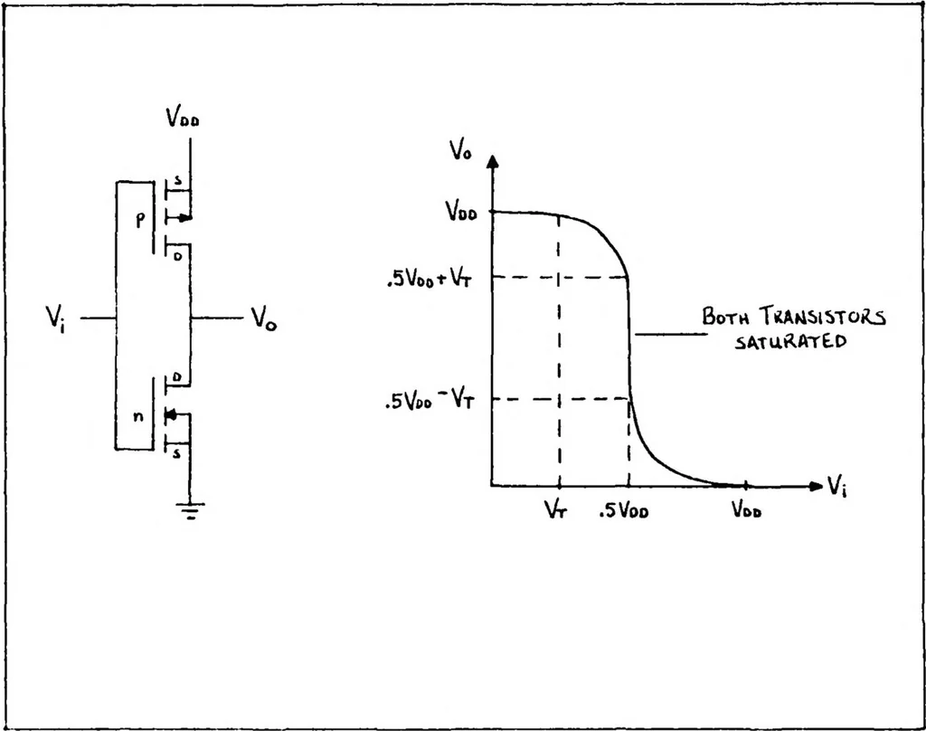
Figure H-2. Typical Inverter and Voltage Transfer Characteristic (7:238,239) transistor requires negative gate-source and drain-source voltages to cause channel formation while the NMOS transistor requires positive gate-source and drain-source voltages. The output voltage, V , is high because it is…
McConkey,M L · Air force inst of tech wright-patterson afb oh school of engineering · Integrated circuits · Metal oxide semiconductors · Simulation · Computer aided design · Theses · Gates(circuits) · Cycles · Bulk materials · Viability · Logic circuits · Logic devices · Flow charting · Circuits · Libraries · Complementary metal oxide semiconductors · Arithmetic units
Internet Archive · Defense Technical Information Center · Public domain (US government work). Free to use for anything.