Inside Out Library · Explore

Computer-Aided Engineering of Semiconductor Integrated Circuits (1979)

Defense Technical Information Center · leaf 223

An illustration from Computer-Aided Engineering of Semiconductor Integrated Circuits, 1979, leaf 223
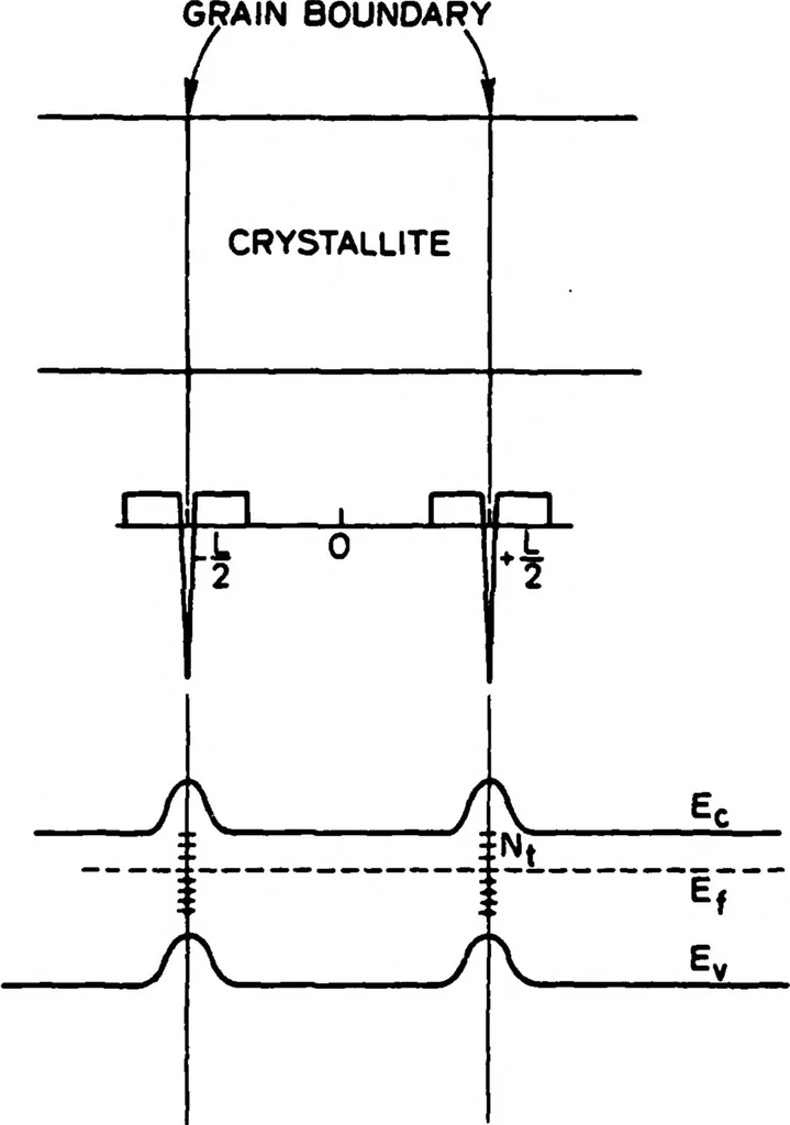
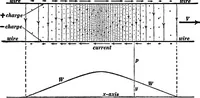
Fig. 3.20. Model of n-type polycrystalllne material showing (a) small crystallites surrounded by grain boundaries containing large numbers of traps, (b) resulting space charge, and (c) corresponding energy-band diagram with potential barriers surrounding the grain boundaries. 217
Meindl, J D · Stanford univ ca integrated circuits lab · Computer aided design · Integrated circuits · Semiconductor devices · Computer applications · Doping · Engineering · Fabrication · Ion implantation · Low costs · Measurement · Military applications · Oxidation · Physical properties · Silicon · Thermal properties · Vapor deposition

Internet Archive · Defense Technical Information Center · Public domain (US government work). Free to use for anything.

More pictures from Computer-Aided Engineering of Semiconductor Integrated Circuits

More like this