Inside Out Library

Computer-Aided Engineering of Semiconductor Integrated Circuits (1979)

Defense Technical Information Center · leaf 373

An illustration from Computer-Aided Engineering of Semiconductor Integrated Circuits, 1979, leaf 373
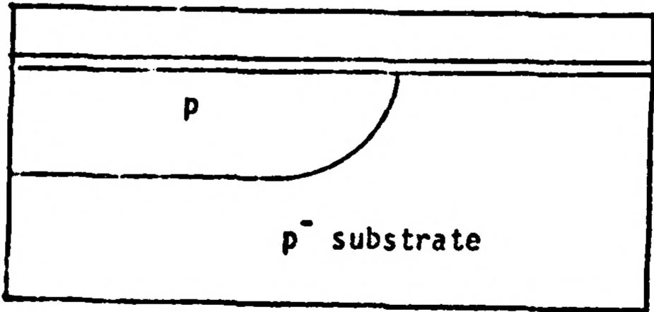
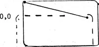
Fig. 4. 6. 34. (a)n-channel MOSFET with nonuniform doping across the width of the channel (x-direction) . (b)surface impurity concentration in x-direction. (c)Threchold VT in x- direction. * U … Fig. 4.6.35. MOS structure for current calculations for coses A, ft and C. A x 10^ Cm-3 N ■;ub G70 A t ox W ■ 20 un 3 2 x U)1CCm'3 N l»t ak 367
Meindl, J D · Stanford univ ca integrated circuits lab · Computer aided design · Integrated circuits · Semiconductor devices · Computer applications · Doping · Engineering · Fabrication · Ion implantation · Low costs · Measurement · Military applications · Oxidation · Physical properties · Silicon · Thermal properties · Vapor deposition

Internet Archive · Defense Technical Information Center · Public domain (US government work). Free to use for anything.

More pictures from Computer-Aided Engineering of Semiconductor Integrated Circuits

More like this