Inside Out Library · Explore

Computer-Aided Engineering of Semiconductor Integrated Circuits (1979)

Defense Technical Information Center · leaf 376

An illustration from Computer-Aided Engineering of Semiconductor Integrated Circuits, 1979, leaf 376
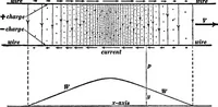
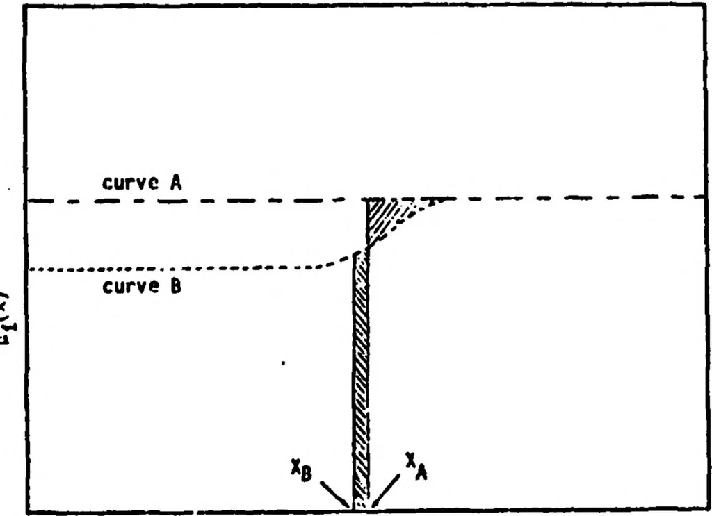
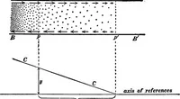
H4 M.« OlSIfiiJCE ( MICRONS ) Fig.4.6.38 Inversion Carrier concentration at several gate potentials calculated by a numerical two-dimensional device simulation program. … Fig. 4.6.391*0 successive approximations for the channel nobility across the device width, »' j C * ) -
Meindl, J D · Stanford univ ca integrated circuits lab · Computer aided design · Integrated circuits · Semiconductor devices · Computer applications · Doping · Engineering · Fabrication · Ion implantation · Low costs · Measurement · Military applications · Oxidation · Physical properties · Silicon · Thermal properties · Vapor deposition

Internet Archive · Defense Technical Information Center · Public domain (US government work). Free to use for anything.

More pictures from Computer-Aided Engineering of Semiconductor Integrated Circuits

More like this